- ▶In the high-end package substrate market as for servers and automotive electronics, mid- to long-term demand is increasing mainly for high multi-layer and large-sized products
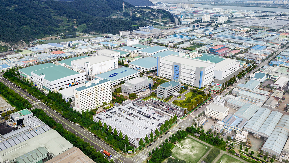
- - SEM invests more in the Busan/Sejong/Vietnam productions of FCBGA, which is recognized for its technological prowess by global top-tier customers
- ▶SEM to strengthen its position as one of the global top three suppliers by mass-producing server package substrates for the first time in Korea within this year
- ▶CEO Chang Duckhyun, “In the future IT environment where AI technologies such as robots, metaverses, and autonomous driving expand, next-generation substrate technologies such as SoS (System on Substrate) will become ‘game changers”
Samsung Electro-Mechanics (SEM) announced on Jun. 22 that it would make an additional investment of KRW about 300 billion to build a package semiconductor substrate (FCBGA) facility.
This investment will be used for facilities of Busan and Sejong plants in South Korea and the production subsidiary in Vietnam, for FCBGA which has been recognized for its technological prowess by global top-tier customers.
With this investment, SEM plans to actively respond to the increase in demand for package substrates due to the high performance and market growth of semiconductors.
Especially through mass-producing server package substrates for the first time in Korea within this year, SEM is strengthening its position as one of the world's top three suppliers by expanding high-end products such as servers, networks, and electronics.
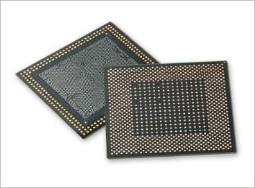
The package substrate, which connects the high-density semiconductor chip and the main board to transmit electrical signals and power, is mainly used in CPU (Central Processing Unit) and GPU (Graphic Processing Unit) that require high-performance and high-density circuit connection.
The semiconductor industry desperately needs the substrate technology that can respond to improvements in semiconductor performance as for robots, metaverses, and autonomous driving. In particular, high-end package substrates required for high-performance fields such as big data and AI involve the highest technical difficulty such as implementation of microcircuits among substrate products, increase in area, and increase in the number of layers.
If the package substrate mounted on a mobile device is compared to an apartment, a high-end type as in a server is equivalent to a skyscraper with more than 100 floors. Because such high technology is required, the business is difficult for latecomers to enter.
In the package substrate market, the demand for high-end products is expected to increase as the performance of servers and PCs improves and the semiconductors for CPU/GPU thereby involve high-performance and multi-chip packaging.
SEM said that the demand for high-end package substrates from global top-tier customers is increasing, and the demand for package substrates for electronic devices is also increasing due to the expansion of autonomous driving.
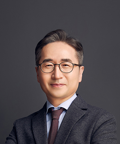
CEO Chang Duckhyun of SEM said, "As AI becomes a core technology in the future IT environment with robots, cloud, metaverse, and autonomous driving, it is becoming very important for manufacturers of high-performance semiconductor such as AI semiconductors to secure partners with the package substrate technology." He added, "SEM will become a 'game changer' in the high-tech field by tapping into the newly conceived package substrate technology such as SoS (System on Substrate)."
SEM started its substrate business in 1991, and is leading the substrate industry by supplying products to major companies in the world. In particular, the company's flagship semiconductor package substrate for mobile AP is unrivaled in market share and technology. The company is the only South Korean substrate maker that has the technology to develop high-end package substrates as for servers. Looking ahead, SEM plans to use its Busan and Sejong production sites and its Vietnamese production subsidiary as outposts for package substrate production to strengthen its customer responsiveness.
※ System on Substrate (SoS)
The role of the post-process of packaging semiconductors is becoming very important in differentiating semiconductor performance as for AI, cloud, and metaverse. As semiconductor performance improves, the number of signal input/output (I/O) increases, which leads to the inevitability of a multi-chip package (MCP) that integrates various functions by arranging two or more semiconductor chips on a substrate.
In the past, substrates played an auxiliary role in semiconductor packaging technology. Lately, however, a substrate
that can cope with multi-chip packages and miniaturization are becoming a key factor in determining overall performance of semiconductors. |